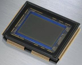
Introduction
conventional solid-state electronic device, method information indicating the presence of, usually with a current or voltage. In the CCD, the charge is, the expression of the CCD information, having a higher sensitivity. The solid imaging, information processing and mass memory are the three main uses of the CCD. Various linear array, the sensor array surface has been successfully used in the field of astronomy, remote sensing, fax, video and other. CCD signal processing both strengths both analog and digital signal processing techniques, widely used in moderate accuracy radar and communications systems. CCD is also used as a large capacity serial access memory, its access time, system capacity and manufacturing costs are between a semiconductor memory and a magnetic disk, drum memory interposed.

principles
1969, the United States Bell Labs WS Boyle and GE Smith in electrical simulation to explore the magnetic bubble devices, resulting in a charge-coupled device principle the idea, and verified in the experiment. They proposed, closely arranged on the semiconductor capacitor insulating surface can be used to store and transfer charge. Initial storage CCD potential wells and transfer signal charges located silicon - silicon dioxide interface, i.e. a so-called surface channel CCD. 1972 D. Kang first conceived of majority carriers in the form of CCD, on this basis, it developed a new channel CCD structure and "creep" type CCD effectively improve the performance of the CCD. In 1973 the United States made Fairchild CCD image sensor, CCD then entered the practical stage from the laboratory to industrial production.
CCD prototype of thin layer of silicon dioxide grown on the N type or P type silicon substrate, and then depositing and lithographically etched silicon dioxide layer on the metal electrodes, which are regularly arranged metal - oxide - semiconductor capacitor array and the appropriate input and output circuitry constitute substantially a CCD shift register. Clock pulse is applied to the metal gate electrode, a potential well is formed can be stored minority carriers in the semiconductor under the corresponding gate electrode. Optical or electrical injection method can be injected charge input signal a potential well. And periodically varying the phase and amplitude of the clock pulse, the potential well depth is correspondingly change over time, so that the signal charge injection orientation for transfer within the semiconductor. CCD output is collected by the reverse biased PN junction charge then amplified, reset, discrete output signals.
charge transfer efficiency is one of the most important performance parameters of CCD, charge amount and the percentage of the total amount of charge transferred by each transfer while FIG. Transfer efficiency limits the maximum transfer CCD of the series.
body channel CCD charge transfer surface channel CCD and the mechanism is slightly different. Body-channel CCD, also known as buried channel CCD. The so-called body and a channel that is used to store the signal charge transfer channel in the surface of the semiconductor body leaving a certain distance. CCD clock frequency of the channel body can be up to several hundred megahertz, and the surface channel CCD typically only a few megahertz.
solid imaging, signal processing and mass memory are the three main uses of the CCD. Various linear array, area array image sensors have been successfully used in the field of astronomy, remote sensing, fax, card readers, optical test television camera and the like, and infrared CCD CCD shimmer underway Yaokong sense, thermal imaging military applications show a significant role. CCD signal processing both strengths both analog and digital signal processing techniques, widely used in moderate accuracy radar and communications systems.
domestic situation
China developed CCD shift register 32 in 1975. China's development work focused on the CCD CCD imaging and signal processing. CCD imager camera has been used in aviation, remote control, industrial automation and other departments. CCD tapped delay line, and an analog delay line play an important role in radar and communications device updates.
