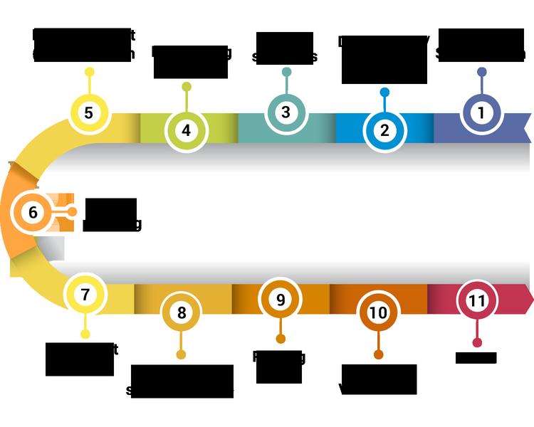
Thedesignincludes
Theflowofintegratedcircuitdesigngenerallyfirstneedstobedividedintosoftwareandhardware,andthedesignisbasicallydividedintotwoparts:chiphardwaredesignandsoftwareco-design.Chiphardwaredesignincludes:
1.Functionaldesignstage.
Designer’sproductapplicationoccasions,setsomespecificationssuchasfunction,operatingspeed,interfacespecifications,environment
environmenttemperatureandpowerconsumption,etc.,asafuturecircuitdesigninaccordancewith.Itcanfurtherplanhowsoftwaremodulesandhardwaremodulesshouldbedivided,whichfunctionsshouldbeintegratedintheSOC,andwhichfunctionscanbedesigned
calculatedonthecircuitboard.
2.Designdescriptionandbehavior-levelverification
Afterthefunctiondesigniscompleted,theSOCcanbedividedintoseveralfunctionalmodulesaccordingtothefunction,andtheIPcoresthatwillbeusedtoimplementthesefunctionsaredetermined.
ThisstageindirectlyaffectstheinternalstructureoftheSOCandtheinteractivesignalsbetweenvariousmodules,aswellasthereliabilityoffutureproducts.
Afterdecidingthemodule,youcanusehardwaredescriptionlanguagesuchasVHDLorVerilogtorealizethedesignofeachmodule.
Then,usethecircuitsimulatorofVHDLorVerilogtoverifythedesign(function
simulation,orbehavioralsimulation).
Notethatthiskindoffunctionalsimulationdoesnotconsidertheactualdelayofthecircuit,norcanitobtainaccurateresults.
3.Logicsynthesis
Afterconfirmingthatthedesigndescriptioniscorrect,youcanusethelogicsynthesistool(synthesizer)forsynthesis.
Inthesynthesisprocess,youneedtoselecttheappropriatelogiccelllibraryasareferencewhensynthesizinglogic

circuits.
Thewritingstyleofthehardwarelanguagedesigndescriptionfileisanimportantfactorthatdeterminestheexecutionefficiencyofthesynthesistool.
Infact,theHDLsyntaxsupportedbysynthesistoolsislimited,andsometooabstractsyntax
isonlysuitableasasimulationmodelforsystemevaluationandcannotbeacceptedbysynthesistools.
Logicsynthesisgetsthegate-levelnetlist.
4.Gate-LevelNetlistVerification
Gate-LevelNetlistVerificationisaregistertransfer-levelverification.Themaintaskistoconfirmwhethertheintegratedcircuitmeetsthefunctionalrequirements.Thistaskisgenerallycompletedwithagate-levelverificationtool.
Notethatthedelayofthegatecircuitneedstobeconsideredinthesimulationatthisstage.
5.Layoutandrouting
Layoutreferstorationallyarrangingthedesignedfunctionalmodulesonthechipandplanningtheirlocations.Wiringreferstothewiringthatcompletestheinterconnectionbetweenmodules.Notethattheconnectionbetweeneachmoduleisusuallyrelativelylong,sotheresultingdelaywillseriouslyaffecttheperformanceoftheSOC,especiallyinthe0.25micronprocessandabove,thisphenomenonismoresignificant.Atpresent,thisindustryisstillavacancyinChina,andtherearestillrelativelyfewuniversitiesofferingintegratedcircuitdesignandintegratedsystems.Amongthem,schoolswithbetterteachersincludeShanghaiJiaotongUniversity,HarbinInstituteofTechnology,HarbinUniversityofScienceandTechnology,SoutheastUniversity,andXi’anElectronicTechnology.University,UniversityofElectronicScienceandTechnologyofChina,FudanUniversity,EastChinaNormalUniversity,etc.Thisfieldhasgraduallybecomesaturated,andthereisagrowingtrendtofollowthepathofthesoftwareindustryinthosedays.
Designprocess
1.Circuitdesign
Completethecircuitdesignaccordingtothecircuitfunction.
2.Pre-simulation
Simulationofcircuitfunctions,includingsimulationofpowerconsumption,current,voltage,temperature,voltageswing,inputandoutputcharacteristicsandotherparameters.
3.Layoutdesign(Layout)
Drawthelayoutbasedonthedesignedcircuit.Cadencesoftwareisgenerallyused.
4.Post-simulation
Simulatethedrawnlayoutandcompareitwiththeprevioussimulation.Ifitfailstomeettherequirements,thelayoutneedstobemodifiedorredesigned.
5.Follow-upprocessing
TheGDSIIfileisgeneratedfromthelayoutfileandsubmittedtoFoundryfortape-out.
